Modeling of Optical Properties of Black Silicon/Crystalline Silicon
Nuggehalli M Ravindra, Sita Rajyalaxmi Marthi,Suramya Sekhri
DOI10.21767/2472-1948.100001
Interdisciplinary Program in Materials Science & Engineering, New Jersey Institute of Technology, Newark, NJ, USA
- Corresponding Author:
- Nuggehalli M Ravindra
Interdisciplinary Program in Materials Science and Engineering, New Jersey Institute of Technology, USA
Tel: 9735963278
E-mail: n.m.ravindra@njit.edu
Received date: October 27, 2015; Accepted date: November 17, 2015; Published date: November 25, 2015
Citation: Ravindra NM (2015) Modeling of Optical Properties of Black Silicon/Crystalline Silicon. J Sci Ind Metrol 1:1. doi: 10.4172/2472-1948.100001
Abstract
Black Silicon, a surface modification of silicon has low reflectance and correspondingly high absorptance in the visible range of wavelengths making it more viable than crystalline silicon for applications in silicon optoelectronics. Like crystalline Si, black silicon has potential applications in solar cells, sensors, antibacterial surfaces and offers new opportunities. In this study, the optical properties of black silicon, in the visible, near and short wavelength infrared region, are simulated based on the effective medium approximation. The application of Helmholtz?s law of optical reciprocity to the two layer medium of black silicon on crystalline silicon is examined. In the long wavelength infrared region, the reported values of emissivity of black silicon are compared with those in the literature. In general, the emissivity of black silicon is higher than that of crystalline silicon.
https://maviyolculuk.online/
https://mavitur.online/
https://marmaristeknekirala.com.tr
https://tekneturumarmaris.com.tr
https://bodrumteknekirala.com.tr
https://gocekteknekirala.com.tr
https://fethiyeteknekirala.com.tr
Introduction
The optical properties of crystalline silicon (c-Si) is one of the most well studied areas in the literature [1] due to its applications in photovoltaics [2], detectors [3], microlenses [4], filters [5] and silicon based optoelectronics [6]. One of the major disadvantages of applications of c-Si in optoelectronics is its significant reflectance (R) and low absorptance (A) in the visible range of wavelengths, in addition to its inherent indirect bandgap [7]. A surface modification of c-Si was introduced in the 1980’s by an unwanted side effect of Reactive Ion Etching (RIE). This modified c-Si had needle-shaped surface structure where needles were made of single-crystal silicon. As a result, the surface of Si appeared black in color, and hence the name “Black Silicon” (b- Si). Black silicon exhibits properties of very low reflectance and high absorptance in both the visible and infrared wavelength regions.
In recent years, several other methods of processing b-Si, such as electrochemical etching [8-10], stain etching [11-19], metalassisted chemical etching using gold nanodots or silver [20-24], laser treatment, etc., have been developed. Of these, the laser treatment of Si has been developed by Eric Mazur and his group at Harvard University [25-30]. As a result of pulsed laser processing, the novel material created has surface texture that facilitates enhanced light absorption. The enhanced light absorption and low reflection of b-Si has prompted b-Si to become an active area of research in renewable sources of energy. Apart from the application of b-Si in solar cells, it has potential applications in image sensors [31], biosensors [32, 33], Micro Electro Mechanical Structures (MEMS) [34], light-emitting devices, antibacterial coatings [35] and gas sensors [36]. B-Si, owing to its high absorptance in the IR region, can be used for IR detection [37]. Photodetectors made of b-Si are expected to have increased sensitivity in the NIR and SWIR range of wavelengths. With the IR sensing properties of b-Si, true digital day-night imaging is possible; this has significant applications in aerospace, defense, security and transportation industries. Recently, a novel method to fabricate black poly-silicon (BPS) has been reported by Fekete et al [38]. In this method, BPS was fabricated on the surface of thermally oxidized Si by RIE at ~ cryogenic temperatures (- 110°C to -90°C). BPS is formed in Low Pressure Chemical Vapor Deposition (LPCVD) deposited poly-silicon thin film by Deep Reactive Ion Etching (DRIE) in the presence of SF6 and O2 plasma at ~ cryogenic temperatures. The potential applications of BPS extend to biological and chemical sensors due to the highly adjustable morphology and integrable fabrication technology. The theory developed in the present study can be extended to BPS by considering its spectral properties.
Experimental Methods in the Literature
Reactive ion etching
This method of producing b-Si uses SF6 and O2 gases to generate free radicals (F* and O*) [39-43]. These free radicals are responsible for etching c-Si, producing volatile products such as SiFx. These products, particularly SiF4, react with the free radicals to form a passivation layer of SiOxFy on a cooled Si surface [41]. Reflectivity can be controlled well by RIE. This way of texturing is ideal for very fragile substrates. The optimal reflectivity of uncontrolled textured cells is around 15% [32].
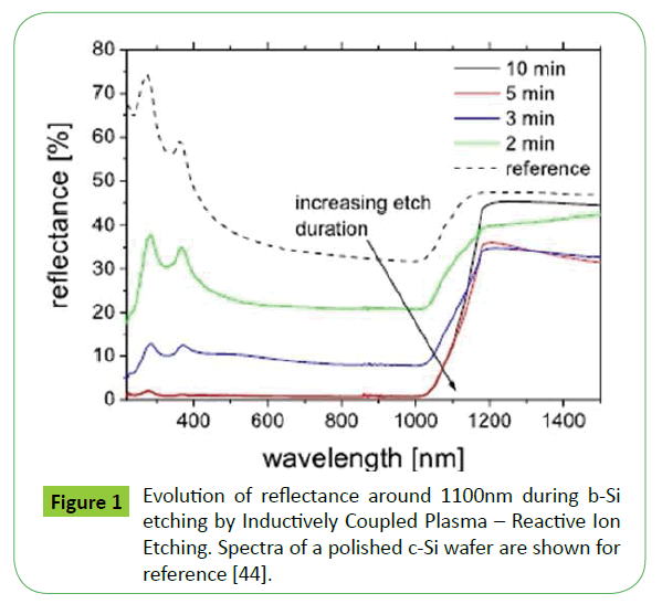
Figure 1 [44], shows the reflectance spectra of the Si samples, in the wavelength range of 200 to 1500nm, etched for different durations. The spectra of polished c-Si before etching are also shown for comparison purposes. It can be observed from the spectra that the optical reflectance spectra of c-Si is reduced significantly right from the onset of structure formation i.e., after 2 mins. The reflectance spectra further decreases with pore growth. After 5 mins, the reflectance spectra are almost completely suppressed and b-Si is formed. The decreased reflectance results in significant increase of absorptance in b-Si [44].
Figure 1: Evolution of reflectance around 1100nm during b-Si etching by Inductively Coupled Plasma – Reactive Ion Etching. Spectra of a polished c-Si wafer are shown for reference [44].
Mazur’s method
A Harvard University group [7] has developed a process in which b-Si is produced by irradiating Si with femtosecond laser pulses. After irradiation of Si surface with a gas containing mixture of SF6/ O2 and other species, the surface of Si develops a self-organized microscopic structure of micrometer-sized cones. Sulfur(S) atoms are forced to the Si surface, creating a structure with a lower bandgap and therefore the ability to absorb longer wavelengths. The excitation of electrons from the bonding to anti-bonding states causes repulsive forces and disorder in the lattice structure while remaining thermally cold [45].
The roughened surface decreases the surface reflection greatly, but the sulfur atoms and structural defects, introduced by laser treatment, create more absorbing states in the sub-band gap region of Si [46,47]. Also, the laser induced damage renders the surface of Si less active electronically [48]. Careful annealing process reduces the number of defects in the Si surface and improves the carrier mobility [28].
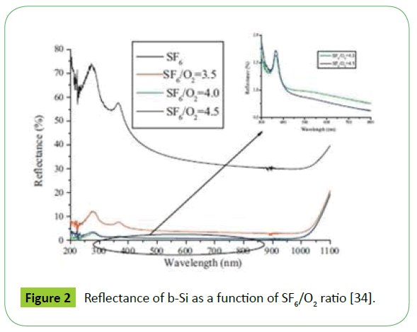
From Figure 2 [34], it can be observed that when only SF6 is used as the plasma gas, the reflectance is very high. There is a significant decrease in reflectance when a mixture of SF6 and O2 is used. This is due to the formation of needle like structures that result in enhanced light trapping. The average reflectance of b-Si over the wavelength range of 200nm to 1100nm is 2.12%. The decrease in reflectance can be explained by diffraction effects in the shorter wavelength range and by moth ball effect in larger range of wavelengths [34].
Figure 2: Reflectance of b-Si as a function of SF6/O2 ratio [34].
Theory & modeling
Optical properties of materials are of importance for a variety of applications. These include applications in non-contact process monitoring and control as well as in the design of coatings, detectors, light emitting devices and waveguides.
Helmholtz’s reciprocity principle
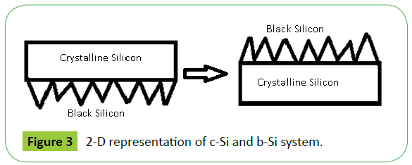
The Helmholtz’s Reciprocity Principle describes the interaction of a ray of incoming light and the corresponding outgoing light with matter. These interactions involve reflections, refractions and absorption in a passive medium or at an interface. The bidirectional reflectance distribution function [49] represents such interactions. The 2-D model of a c-Si and b-Si system, considered for examining the reciprocity principle, in this study, is shown in Figure 3.
Effective medium approximation
The effective medium approximation [50,51] is based on an assumption that an inhomogeneous material is composed of two types of spherical grains with complex-valued permittivity, ε1 and ε2, mixed in volume fractions of (f) and (1-f) [52, 53] where, f is the volume filling factor. The derivation of effective permittivity ε* is based on the assumption that allows to replace the material surrounding the inclusions by a homogeneous matrix material with the same effective permittivity ε*(f, ε1, ε2). First order approximation is used to calculate the resulting effective property for the dilute composite.
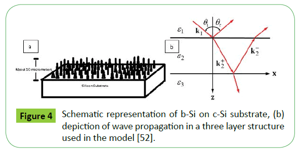
We consider a layer of vertically aligned b-Si array on a semiinfinite Si substrate, as shown in Figure 4 [52]. It should be noted that the assumption of the Si substrate being treated as opaque is a good one because the penetration depth of Si is usually small, except at wavelengths close to the indirect bandgap (around 1.1 μm wavelength). The basic assumption is that the characteristic geometric dimensions are much smaller than the wavelength of the electromagnetic waves.
Figure 4: Schematic representation of b-Si on c-Si substrate, (b) depiction of wave propagation in a three layer structure used in the model [52].
Based on Bruggeman’s effective medium approximation, the effective dielectric function εeff of the b-Si layer can be calculated by solving the following equation:
 (1)
(1)
where, εair and εSi are the dielectric functions of air and Si respectively. The depolarization factor g depends on the geometry and polarization.
In order to simulate the wavelength dependent optical properties of the multi-layers and its reciprocity, i.e., c-Si/b-Si and b-Si/c-Si, we use Multi-Rad.
Multi-rad
Multi-Rad was created at Massachusetts Institute of Technology by Hebb et.al. [54]. Multi-Rad is a PC- based modelling software that enables the calculations of the radiative properties of thinfilm stacks, with emphasis on semiconductor applications. The matrix method of multi layers forms the basis of the calculations. This model assumes that the layers are optically smooth and parallel and that the materials are optically isotropic. Thus the interfaces are considered to be abrupt. For a given multilayer stack, at specific temperature, wavelength and angle of incidence dependent radiative properties are obtained.
The radiative properties of the multilayer stacks are calculated using the matrix method of multilayers [55-57]. Radiation at a given wavelength is treated as coherent; therefore, interference effects are taken into account. The main assumption of the theory is that the layers are parallel and optically isotropic, the surface is optically smooth, and the area of the multilayer stack is much larger than the wavelength of the incident radiation.
Thermal radiation is usually well approximated as unpolarized. The directional transmittance and reflectance are calculated as simple average of s and p wave properties. This theory makes it general such that the predicted properties do not depend on classifying the radiation in a layer as coherent or incoherent.
The spectral absorptance (A) is calculated from:
A(λ) = 1- R(λ)-T(λ) (2)
It should be noted that the measurement of the optical properties, in the infrared range of wavelengths, is complex. This is in spite of the significant development in instrumentation relating to these measurements. In particular, the estimation of the wavelength dependent extinction coefficient, k, and its reported values in the literature are sparse and sometimes, in a wide range, for the same wavelength. The measurement becomes more complicated for rough surfaces, multi-layers and highly infrared transparent materials. While spectral emissometry [58] provides a methodology for hemispherical measurements of the optical properties, Fourier Transform Infrared Spectrophotometry (FTIS) has become a standard tool for such measurements [59].
Kirchhoff’s law
In general, any object at a temperature T radiates electromagnetic energy. A perfect black body in thermodynamic equilibrium absorbs all light that strikes it, and radiates energy according to the law of radiative emissive power for temperature T, universal for all perfect black bodies. Kirchhoff's law [60] states that:
“for an object of any arbitrary material, emitting and absorbing thermal electromagnetic radiation at every wavelength in thermodynamic equilibrium, the ratio of its emissive power to its dimensionless coefficient of absorption is equal to a universal function only of radiative wavelength and temperature, the perfect black-body emissive power.”
In other words, Kirchhoff’s law describes the optical reflectance reciprocity as a material or structural property. The reflectance of an optical system is measured by detecting the light reflected off of the system when a source of light is incident on the system. If reciprocity holds for the material, the detector response is the same when the source and detector positions are switched.
Emissivity
Emissivity (Є) of the surface of a material is its effectiveness in emitting energy as thermal radiation. All objects do not radiate infrared (thermal) energy equally. An ideal black body has an emissivity of 1.0 and no other material can radiate more thermal energy at a given temperature. Materials have value of ? between 0 and 1. The emissive and reflective behavior of most materials is similar in the visible and IR regions. However, some materials may differ in their emissive and reflective behavior.
Hemispherical Emissivity:
 (3)
(3)
where,
Me – radiant flux emitted by the surface
Moe – radiant flux emitted by a black body at the same temperature as the surface.
Directional Emissivity:
 (4)
(4)
Where,
Le, Ω – radiant flux emitted by the surface
Loe, Ω – radiant flux emitted by a black body at the same temperature as the surface.
For the modeling purposes in this study, the samples considered are b-Si coated on c-Si wafers of 200 mm diameter (usually referred to as "8 inch"), thickness 725 μm. The doping is p-type with dopant concentration of 1 x 1016 cm-3. The thickness of b-Si is varied in the range of 1 – 10 μm. In order to investigate the reciprocity in the optical properties, R, T and A of c-Si/b-Si are compared, with those of b-Si/c-Si, for b-Si thickness of 5 μm, in Table 1.
| λ (µm) | Reflectance | Transmittance | Absorptance | ||||||
|---|---|---|---|---|---|---|---|---|---|
| c-Si | c-Si/b-Si | b-Si/c-Sib-Si | c-Si | c-Si/b-Si | b-Si/c-Sib-Si | c-Si | c-Si/b-Si | b-Si/c-Sib-Si | |
| 0.5 | 0.385 | 0.385 | 0.19 0.018 | ~0 | ~0 | ~0~0 | 0.615 | 0.615 | 0.91 0.980 |
| 1.0 | 0.318 | 0.318 | 0.0230.027 | 0.001 | ~0 | ~0~0 | 0.681 | 0.682 | 0.977 0.973 |
| 1.1 | 0.269 | 0.260 | 0.0340.034 | 0.424 | 0.029 | 0.029 0.028 | 0.307 | 0.711 | 0.937 0.938 |
| 1.2 | 0.477 | 0.404 | 0.0430.045 | 0.521 | 0.035 | 0.0350.035 | 0.002 | 0.561 | 0.922 0.920 |
| 1.5 | 0.471 | 0.391 | 0.030 0.032 | 0.525 | 0.029 | 0.029 0.028 | 0.004 | 0.580 | 0.941 0.940 |
| 2.0 | 0.453 | 0.402 | 0.0270.024 | 0.541 | 0.037 | 0.037 0.046 | 0.006 | 0.561 | 0.936 0.930 |
| 2.4 | 0.447 | 0.383 | 0.0380.038 | 0.545 | 0.045 | 0.045 0.042 | 0.008 | 0.572 | 0.917 0.920 |
Table 1: Summary of optical properties of c-Si, b-Si/c-Si and c-Si/b-Si in comparison with b-Si.
Results and Discussion
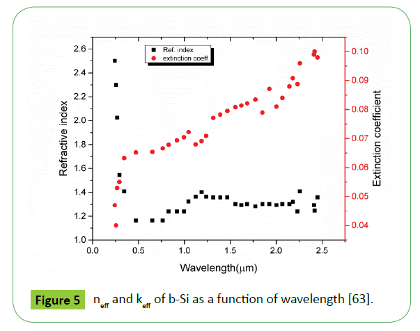
The unique features of b-Si – improved light trapping and decreased reflectance make it an ideal candidate for solar cell applications. The low reflectance of b-Si indicates that the refractive index is lower than that of c-Si. Just as in the case of porous silicon (p- Si) [59, 61, 62], the effective medium approximation [50-51] can be used to determine the optical constants of b-Si. The optical constants thus obtained are effective refractive index (neff) and effective extinction coefficient (keff).
Figure 5 [63] illustrates the optical constants, i.e., the effective refractive index and effective extinction coefficient of b-Si obtained by using the effective medium approximation. An abrupt change in the extinction coefficient in the wavelength range of 900 – 1100 nm is observed; this corresponds to the energy gap of crystalline silicon.
Figure 5: neff and keff of b-Si as a function of wavelength [63].
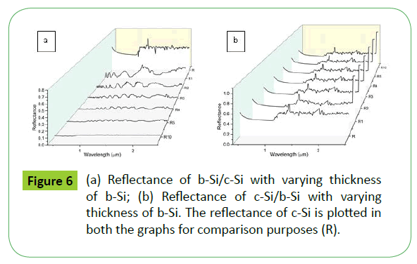
From Figure 6(a), for b-Si/c-Si, it can be seen that with increase in thickness of b-Si layer, the reflectance of the sample is strongly influenced. For 10 micron thick b-Si layer, the reflectance is below 1% (R10), and is very close to zero. In Figure 6(b), for c-Si/b-Si, there is no effect of change in thickness of b-Si on the reflectance of the multilayer. Since reflectance is a surface property, it remains the same as that of c-Si. In the lower wavelength region, i.e., from 0.4 to 1.0 μm, the reflectance of c-Si/b-Si sample is almost uniformly changing. Beyond the wavelength of 1.1 μm, the reflectance behaves similarly with change in wavelength. The fluctuations in R are the result of interference effects.
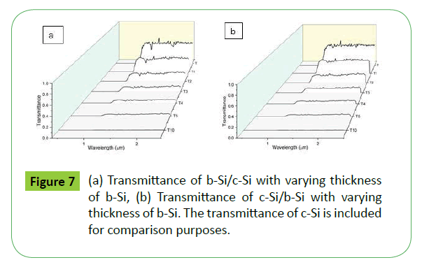
By comparing Figures 7(a) and 7(b), we observe that the transmittance for b-Si/c-Si and c-Si/b-Si are the same and behave similarly with wavelength. With increase in thickness of b-Si, the transmittance decreases. The transmittance becomes almost zero when the thickness of b-Si is 5μm (T5) and is ~ zero for samples with 10 μm (T10) thick b-Si, throughout the entire range of wavelengths considered in this study. Though the influence of b-Si on the reflectance of c-Si/b-Si is negligible [Figure 6(b)], the transmittance is affected by the presence of b-Si in c-Si/b-Si [Figure 7(b)]. In the region of the energy gap of c-silicon (1.1μm), there is a change in the transmittance which becomes less pronounced as the thickness of b-Si layer increases [Figure 7(b)].
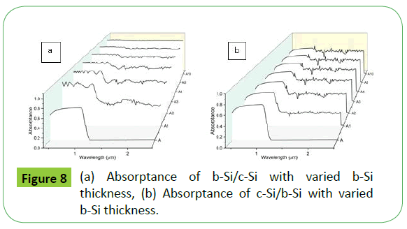
From Figure 8(a), it is clear that b-Si has positive effect on the absorptance. As the thickness of b-Si increases, the absorptance of b-Si/c-Si increases and approaches almost unity [Figure 8(a)]. Though the change in the absorptance with respect to wavelengths below the energy gap (1.1 μm) is very small, the absorptance in the wavelength regions beyond the energy gap has improved. However, in the case of c-Si/b-Si, the influence of varying thickness of b-Si is minimal [Figure 8(b)]. The influence of interference effects and diffraction effects is less prominent in the lower range of wavelengths.
In these calculations, all the values of reflectance, transmittance and absorptance are approximated to 3 decimal places. In Table 1, a comparison of the R, T and A of c-Si/b-Si and b-Si/c-Si, with respect to c-Si is presented. The thickness of b-Si, considered in this comparison in Table 1, is 5 microns. The R for c-Si/b-Si is higher than that of b-Si/c-Si. Correspondingly, A for c-Si/b-Si is lower than that of b-Si/c-Si. This result is independent of the wavelengths considered in this study.
In Table 2, the emissivity values of n type Si and b-Si, from the literature, are compared for selected long wavelengths in the infrared. As can be seen in this table, the emissivity of b-Si is generally higher than that of n-Si. The emissivity of b-Si decreases with increasing temperature. Due to free carrier absorption, the emissivity of n-Si, increases with increase in temperature. At higher temperatures and longer wavelengths, the emissivity of n-Si is higher than that of b-Si (T = 873 K, 973 K; Wavelength = 12.5 μm, 15.0 μm).
| Wavelength (µm) |
Emissivity | Emissivity | ||
|---|---|---|---|---|
| n- Si* (543K) |
b-Si (473K) |
n- Si* (873K) |
b-Si (973K) |
|
| 5.0 | 0.06 | 0.90 | 0.70 | 0.83 |
| 7.5 | 0.20 | 0.89 | 0.70 | 0.83 |
| 10.0 | 0.30 | 0.88 | 0.68 | 0.74 |
| 12.5 | 0.45 | 0.86 | 0.68 | 0.63 |
| 15.0 | 0.53 | 0.82 | 0.68 | 0.54 |
| 17.5 | 0.78 | 0.51 | ||
| 20.0 | 0.74 | 0.46 | ||
| 22.5 | 0.68 | 0.42 | ||
| 25.0 | 0.56 | 0.43 | ||
Table 2: Emissivity of b-Si and n-Si* with source at various temperatures [64, 65].
From a solar cell perspective, the National Renewable Energy Laboratory (NREL) has reported the best efficiency of b-Si solar cell; the reported efficiencies are 16.8% [64-66] and 18.2% [67]. Based on the decrease in reflectance losses of b-Si, the anticipated improvement in efficiency, assuming the device performance to be similar to that of c-Si [68], should be about 30%.
Conclusion
Optical properties of black silicon have been investigated in the above study. Effective medium approximation and the Helmholtz’s optical reciprocity have been examined for a two layer model that consists of black silicon and crystalline silicon. The results show significant differences in reflectance and absorptance for this two-layer model. Comparison of the emissivity of n-Si and b-Si, in the infrared long wavelength range, has been presented.
References
- Ravindra N M, Narayan J (1986) Optical properties of amorphous silicon and silicon dioxide. J ApplPhys 60: 1139-46.
- Singh P, Ravindra N M (2012) Temperature dependence of solar cell performance—an analysis. Solar Energy Materials and Solar Cells 101:36-45.
- Lepselter M P, Fiory A T , Ravindra N M (2008) Platinum and Rhodium silicide – Germanium Optoelectronics. Journal of Electronic Materials 37: 403-416.
- Ravindra N M, Tong F M, Pattnaik D K, Ivanov D I, Levy R A, et al. (1998) Silicon microlenses for IR image sensors.Proc. SPIE 3511, Micromachining and Microfabrication Process Technology IV 152.
- Tong F M, Ravindra N M, Kosonocky W F (1998)Design and simulation of permissible tolerance during fabrication of infrared-induced transmission filters. Opt. Eng. 36: 549-57.
- Fiory A T, Ravindra N M (2003) Light emission from silicon: some perspectives and applications. Journal of Electronic Materials 32: 1043-1051.
- FilippoFabbri, Yu-Ting Lin, Giovanni Bertoni, Francesca Rossi, Matthew J. Smith, et al. (2015) Origin of the visible emission of black silicon microstructures. Applied Physics Letter. 107: 1-7.
- Lie L H, Duerdin M, Tuite E M, Houlton A, Horrocks B R (2008) Preparation and characterization of luminescent alkylated-silicon quantum dots. J Electroanal. Chem538: 183–190.
- Chao Y, Siller L, Krishnamurthy S, Coxon P R, Bangert U, et al. (2007)Evaporation and deposition of alkyl-capped silicon nanocrystals in ultrahigh vacuum. Nat. Nanotechnol. 2:486–489.
- Ahire J H, Wang Q, Coxon P R, Malhotra G, Brydson R, et al. (2012)Highly luminescent and nontoxic amine-capped nanoparticles from porous silicon: synthesis and their use in biomedical imaging. ACS Appl. Mater. Interfaces 4:3285–3292.
- Tsakalakos L, Balch J, Fronheiser J, Korevaar B, Sulima O, et al. (2007) Silicon nanowire solar cells. Appl. Phys. Lett. 91: 1- 3.
- Smith R, Collins S (1992) Porous silicon formation mechanisms. J. Appl. Phys71: R1–R22
- Saadoun M, Mliki N, Kaabi H, Daoudi K, Bessais B, et al. (2002) Vapour-etching-based porous silicon: a new approach. Thin Solid Films 405:29–34.
- Rabha M B, Dimassi W, Bouäicha M, Ezzaouia H, Bessais B (2009) Laser-beam-induced current mapping evaluation of porous silicon-based passivation in polycrystalline silicon solar cells Sol. Energy 83:721–725.
- Ben Rabha M, Saadoun M, Boujmil M, Bessais B, Ezzaouia H, et al. (2005) Application of the chemical vapor-etching in polycrystalline silicon solar cellsAppl. Surf. Sci. 252:488–493.
- Ben Jaballah A, Hassen M, Hajji M, Saadoun M, Bessais B, et al. (2005)Chemical vapour etching of silicon and porous silicon: silicon solar cells and micromachining applications. Phys. Status Solidi A 202:1606–1610.
- Jaballah A B, Saadoun M, Hajji M, Ezzaouia H Bessäis B (2004)Silicon dissolution regimes from chemical vapour etching: from porous structures to silicon grooving. Appl. Surf. Sci. 238:199–203.
- Saadoun M, Bessäis B, Mliki N, Ferid M, Ezzaouia H, et al. (2003)Formation of luminescent (NH4)2SiF6 phase from vapour etching-based porous silicon. Appl. Surf. Sci. 210:240–248.
- Rabha M B, Anouar H, Brahim B (2012) Improvement of multicrystalline silicon solar cell performance via chemical vapor etching method-based porous silicon nanostructures. Sol. Energy 86:1411–1415.
- Li X, Bohn P (2000) Metal-assisted chemical etching in HF/H2O2 produces porous silicon. Appl. Phys. Lett.77:2572–2574.
- Huang Z, Geyer N, Werner P, De Boor J, Gösele U (2011) Metal-Assisted Chemical Etching of Silicon: A Review.Adv. Mater. 23: 285–308.
- Srivastava S K, Kumar D, Singh P K, Kar M, Kumar V, et al. (2010) Excellent antireflection properties of vertical . silicon.nanowire . arrays . Sol.Energy . Mater . Sol . CellS94 : 1506 – 1511.
- Koynov S, Brandt M S, Stutzmann M (2006) Black nonreflecting silicon surfaces for solar cells.Appl. Phys. Lett. 88:1 - 3.
- VorobyevA Y, Guo C (2013)Direct femtosecond laser surface nano/microstructuring and its applications.Laser Photonics Rev. 7:385–407.
- Her T H, Finlay R J, Wu C, Deliwala S, Mazur E (1998) Microstructuring of silicon with femtosecond laser pulses. Applied Physics Letter 73:1673-1675.
- Her T H, R J Finlay, Wu C, Mazur E (2000) Femtosecond laser – induced formation of spikes on silicon.Appl. Phys. A: Mater. Sci. Process. 70:383–385.
- Wu C, Crouch C, Zhao L, Carey J, YounkinR,et al. (2001)Near-unity below-band gap absorption by microstructured silicon. Appl. Phys.Lett. 78:1850–1852.
- Carey J E, Warrender J M, Aziz M J, Mazur E, et al. (2004) Infrared absorption by sulfur-doped silicon formed by femtosecond laser irradiation Applied Physics Letter 84: 1635-1641.
- Sarnet T, Derrien T, R Torres, Delaporte P, Torregrosa F,et al. (2012)From black silicon to photovoltaic cells, using short pulse lasers Proceedings of 28th European Photovoltaic Solar Energy:219 -228.
- Sarnet T, Derrien T, Torres R, Delaporte Ph., Torregrosa F,et al. (2013) Black silicon for photovoltaic cells: towards a high-efficiency silicon solar cell.Conference and Exhibition, Paris: 1882–1886.
- Liu X, Coxon P R, Peters M, Hoex B, Cole J M, et al. (2014) Black silicon: fabrication methods, properties and solar energy. Energy Environmental Science 7: 3223-3263.
- Dekkers H F W, Duerinckx F, Szlufcik J, J Nijs (2000) Silicon surface texturing by reactive ion etching. Opto-Electronics Review 8: 311-316.
- BercesZs, Horvath A,Jady A, Pongracz A, Madrasz E, et al. (2014) Neural cell response to nanostructured biosensor surfaces. Proc. Eng. 87:971-974.
- Xia Y, Liu B, Zhong S, Li C (2012) X-ray photoelectron spectroscopic studies of black silicon for solar cell. Journal of Electron Spectroscopy and Related Phenomena 184: 589-592.
- Ivanova E P, Hasan J, Webb H K, Gervinskas G, Juodkazis S, et al. (2013) Bactericidal activity of black silicon. Nature Communications 4: 2838-2848.
- Jimenez- Cadena G, Riu J, Rius F X (2007) Gas sensors based on nanostructured materials. Analyst 132:1083-1099.
- Carey J E, Sickler J (2009) Black Silicon sees further into the IR, article in Laser Focus World in August 2009, 40 – 44.
- Fekete Z, Horvath A Cs, BercesZs, Pongacz A (2014) Black poly-silicon: A nanostructured seed layer for sensor applications. Sensors and Actuators A 216: 277-286.
- Jansen H, de Boer M, Legtenberg R, Elwenspoek M (1995) The black silicon method: a universal method for determining the parameter setting of a fluorine-based reactive ion etcher in deep silicon trench etching with profile control. J.Micromech. Microeng. 5:115–120.
- Dussart R, Tillocher T, Lefaucheux P, Boufnichel M (2014)Plasma cryogenic etching of silicon: from the early days to today's advanced technologies.J.Phys. D: Appl. Phys.47:1 – 27.
- Drussart R, Boufnichel M, Marcos G, Lefaucheux P, Basillaus A, et al. (2004) Passivation mechanism in cryogenic SF6/O2 etching process. J.Micromech. Microeng. 14:190-196.
- Dussart R, Mellhaoui X, Tillocher T, Lefaucheux P, Boufnichel M , et al. (2007) The passivation layer formation in the cryo-etching plasma process. Microelectron. Eng. 84: 1128-1131.
- Dussart R, Mellhaoui X, Tillocher T, Lefaucheux P, Volatier M, et al. (2005) Silicon columnar microstructures induced by an SF6/O2 plasma. J.Phys. D: Appl. Phys. 38: 3395-3402.
- Steglich M, Käsebier T, Zilk M, Pertsch T, Kley E-B, et al. (2014) The structural and optical properties of black silicon by inductively coupled plasma reactive ion etching. Journal of Applied Physics 116: 1-12.
- Sundaram S, Mazur E (2002) Inducing and probing non-thermal transitions in semiconductors using femtosecond laser pulses.Nature Materials 1: 217-24.
- Wu C, Crouch C H, Zhao L, Carey J E, Youkin R, et al. (2001) Near-unity below-band-gap absorption by micro-structured silicon. Applied Physics Letter 78:1850-1852.
- Carey J E, Crouch C H, Shen M, Mazur E (2005) Visible and near-infrared responsivity of femtosecond-laser microstructured silicon photodiodes.Optics Letters 30: 1773-1775.
- Lü Q, Wang J, Liang C, Zhao L, Jiang Z (2013)Strong infrared photoluminescence from black silicon made with femtosecond laser irradiation. Opt. Letter 38: 1274-1276.
- Hapke B (2012) Theory of reflectance and emittance spectroscopy, Cambridge University Press, Cambridge, UK.
- Khardani M, Bouaïcha M, Bessaïs B (2007) Bruggeman effective medium approach for modelling optical properties of porous silicon: comparison with experiment. Physics Status Solidi (c) 4:1986-1990.
- D. Stroud (1998) The effective medium approximations: Some recent developments.Superlattices and Microstructures 23: 567-73.
- Wang H, Liu X, Wang L, Zhang Z (2013) Anisotropic optical properties of silicon nanowire arrays based on the effective medium approximation. International Journal of Thermal Sciences 65: 62-69.
- Zhang D, Cherkaev E, Lamoureux M P (2011) Stieltjes representation of the 3D Bruggeman effective medium and Pade approximation. Applied Mathematics and Computation 217: 7092-7107.
- Hebb J, Jenson K F (1996) The Effect of Multilayer Patterns on Temperature Uniformity during Rapid Thermal Processing. J. Electrochem. Soc. 143: 1142-1151.
- Hebb J P, Jenson K F (1997) User’s Manual Multi-Rad Version 1.0 Massachusetts Institute of Technology Cambridge MA.
- Katsidis C C, Siapkas D I (2002) General transfer-matrix method for optical multilayer systems with coherent, partially coherent, and incoherent interference. Applied Optics 41: 3978-3987.
- Santberg R, Smets A H M, Zeman M (2013) Optical model for multilayer structures with coherent, partly coherent and incoherent layers. Optics Express 21: 62-67.
- Ravindra N M, Abedrabbo S, Chen W, Tong F M, Nanda A K, et al. (1998) Temperature-dependent emissivity of silicon-related materials and structures. IEEE Transactions on Semiconductor Manufacturing 11: 30-39.
- Hanssen L, Kaplan S, Datla R (2015) Infrared Optical properties of materials, Natl. Inst. Stand. Technol. Spec. Publ. 250-294.
- Kirchhoff G (1860) Ueber das VerhältnisszwischendemEmissionsvermögen und demAbsorptionsvermögen der KörperfürWärme and Licht. Annalen der Physik und Chemie185: 275-301.
- Golovan L A, Timoshenko V Y (2003) Nonlinear-optical properties of porous silicon nanostructures. Journal of Nano electronics and Opto electronics 8: 223-39.
- Singh P, Sharma S N, Ravindra N M (2010) Applications of porous silicon thin films in solar cells and biosensors. JOM 16:15-24.
- SitaRajyalaxmi M, Suramya S, Ravindra N M, (2015) Optical properties of black silicon – An analysis. JOM 67: 2154-2159.
- Maloney P G, Smith P, King V, Billman C, Winkler M, et al. (2010) Emissivity of microstructured silicon. Applied Optics 49: 1065-68.
- Ravindra N M, Sopori B, Gokce O H, Cheng S X, Shenoy A, et al. (2001) International Journal of Thermophysics 22: 1593 – 1611.
- Yuan H C, Yorst V E, Page M R, Stradins P, Meier D L, et al. (2009) Efficient black silicon solar cell with a density-graded nanoporoussurface:Optical properties, performance limitations, and design rules. Appl. Phys. Lett. 95:1 – 3.
- Oh J, Yuan H C, Branz H M (2012) An 18.2% efficient black-silicon solar cell achieved through control of carrier recombination in nanostructures. Nature Nanotechnology 7:743-748.
- Shockley W, Queisser H J (1961) Detailed balance limit of efficiency of pn junction solar cells. J. Appl. Phys. 32:510-519
Open Access Journals
- Aquaculture & Veterinary Science
- Chemistry & Chemical Sciences
- Clinical Sciences
- Engineering
- General Science
- Genetics & Molecular Biology
- Health Care & Nursing
- Immunology & Microbiology
- Materials Science
- Mathematics & Physics
- Medical Sciences
- Neurology & Psychiatry
- Oncology & Cancer Science
- Pharmaceutical Sciences
